IKCH-58 Universal Adaptor Boards
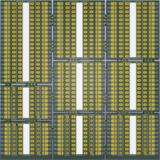
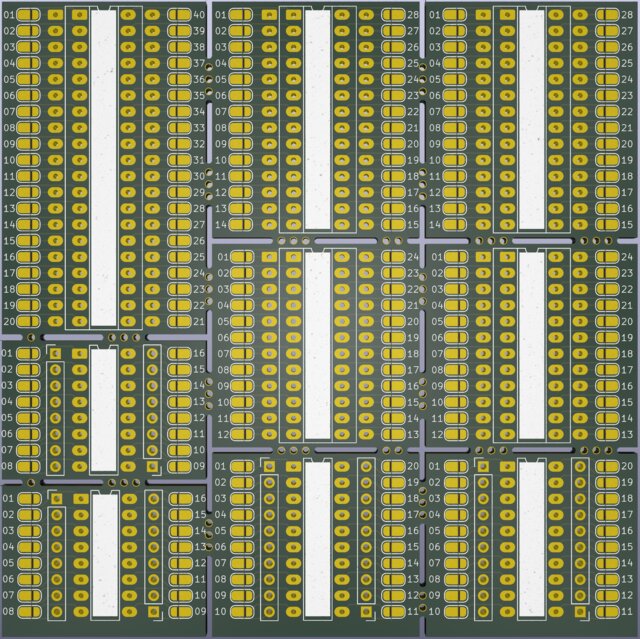
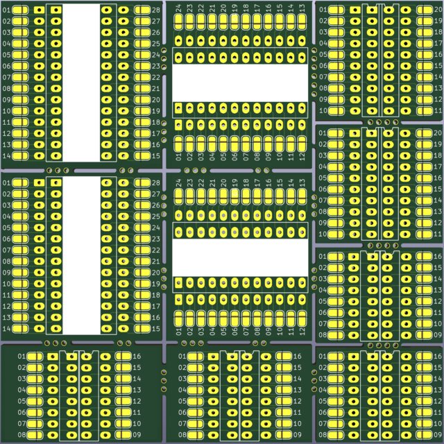
The IKCH58 Universal Adaptor Boards consists of 9 or 10 separate PCBs that can be snapped apart to produce individual 16, 20, 24, 28, and 40 pin adaptor boards.
The REV A boards are intended for use "over" an existing IC (and thus have unusual socket width sizes), whereas the REV B boards are intended for use "offset" from an existing IC.
Each board consists of two sets of connectors, a top half and a bottom half.
The top half connector is intended to host the "chip being adapted" (CBA), whereas the bottom half connector hosts the "ideal chip presentation" (ICP).
My use case for the REV A boards is for use with my IC tester, which has a few basic assumptions about the pinout:
- VCC (be it +3V3 or +5V) is always on the right top-most pin, and
- GND is always on one of pins {7, 8, 9, 10, 12, 14, 16, or 20}.
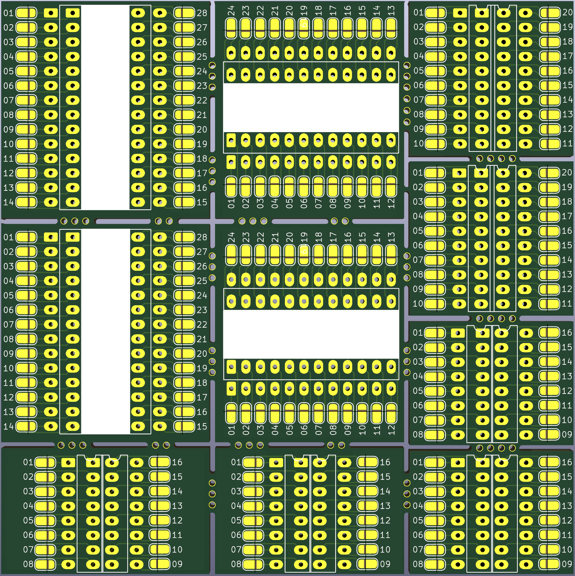
The CBA, however, usually has different views on where power goes. The chip that motivated this particular effort is the 68B50 UART. It's a 24 pin DIP that helpfully puts VCC on pin 12, and GND on pin 1.
So, using the 24-pin IKCH58A universal adaptor board, I can basically wire most of the pins as "through" connections, and I just need to move VCC (pin 12) to -CTS (pin 24), and swap VSS (pin 1) with -CTS (pin 24). That is, I move -CTS to pin 1, VSS to pin 12 (like the universe intended), and VCC to pin 24 (also, much like the universe intended).
This is three wires, and one adaptor, which now means that I can test the 68B50 UART (modulo writing some actual test sotware for it).
Connector Weirdness on the REV A
You may have noticed that there are wide chips and narrow chips. A 40-pin chip is 0.6" wide, whereas a 16-pin chip is 0.3" wide. My IC tester has a ZIF socket that can accomodate an up-to 40-pin chip, with widths between 0.3" and 0.6".
So, the adaptor for the 40-pin chip (top left in the REV A board picture), has a 0.6" socket on top, and 0.3" dual row pin headers on the bottom. This presents an "oddly shaped" 40-pin chip to the IC tester (that is, it presents a 40-pin 0.3" wide chip, which just doesn't exist in nature). On the other hand, the 16-pin chip adaptor (bottom left), has a 0.3" socket on top, and 0.6" dual row pin headers on the bottom. It too presents an oddly shaped 16-pin 0.6" wide chip, also something you don't see in the wild. Best of both worlds.
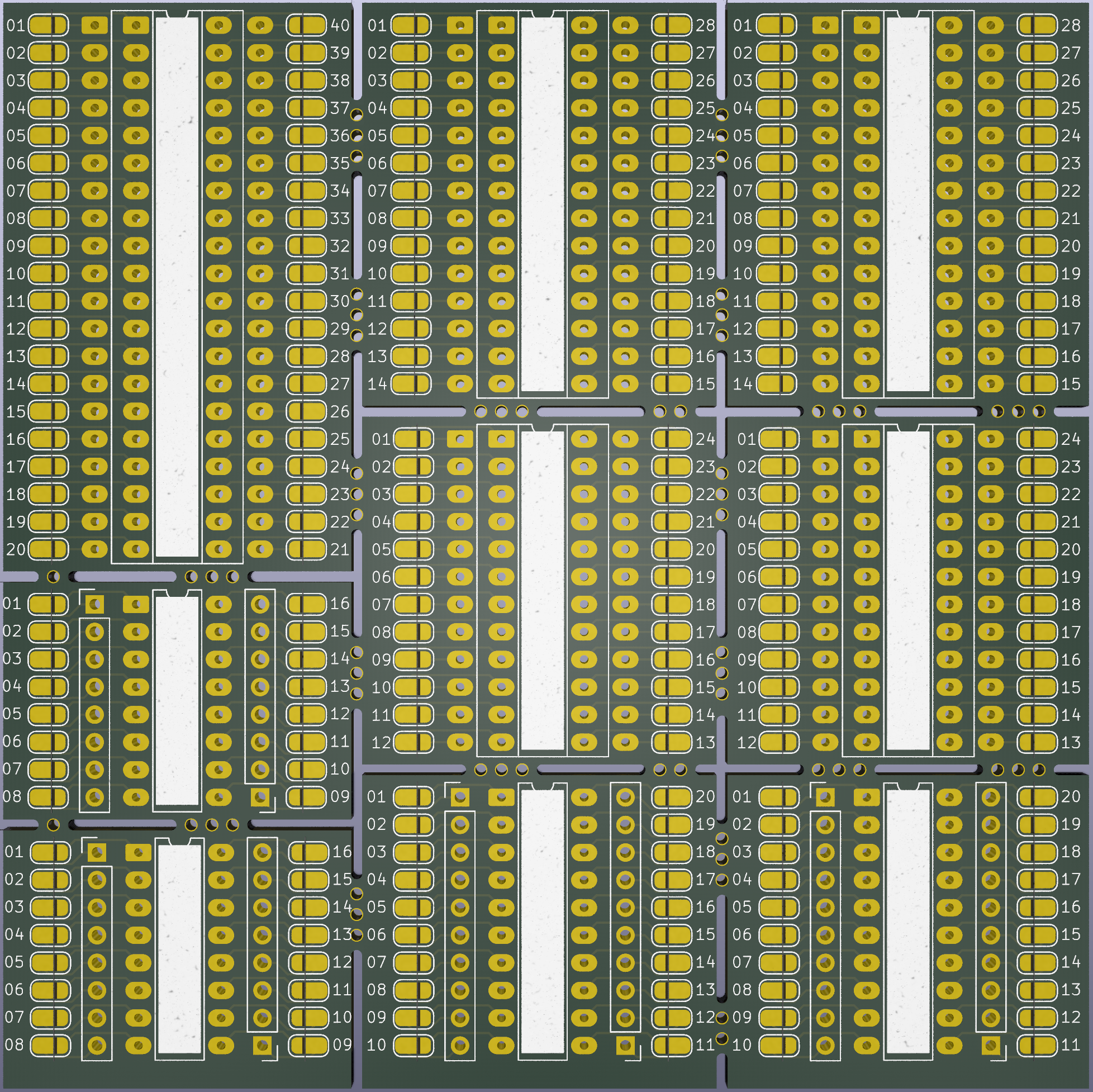
Patch area
For each pin, you have the option of putting in a solder jumper (basically, you're saying that you like the pin where it is, connect it through), or you can kludge a wire jumper. The outer part of the connector is the target pin (ICP), the inner part of the connector is the source pin (CBA).
So, if you want to effect the 68B50 UART adaptor, you'd use the 24-pin adaptor, and wire as follows:
- solder jumper on every pin except 1, 12, and 24.
- connect outer pin 1 to inner pin 24.
- connect outer pin 12 to inner pin 1.
- connect outer pin 24 to inner pin 12.
The first step, soldering every jumper connection expcet the three pins, provides connectivity to all of the pins that remain the same between ICP and CBA.
The second step connects the ICP pin 1 to CBA pin 24. Consulting the data sheet, pin 24 of the 68B50 is the -CTS pin — so we're effectively moving that pin to appear on pin 1.
The third step connects ICB pin 12 to CBA pin 1. This effectively moves the GND (presented on ICB pin 12) to where it is on the chip (pin 1).
Finally, the fourth step connects ICB pin 24 to CBA pin 12. This moves VCC (presented on ICB pin 24) to where it is on the chip (pin 12).
Effectively, we've transposed three pins on the CBA to their ICP versions, and left the other 21 pins alone.
REV B
The REV B versions adapt the CBA to the ICP but preserve the pin spacing.