IKCH-55 Dual PICO-Based IC Tester
I recently designed a 9 position rotary encoder board, and soldered in a CD4028B chip to decode select lines for each of the rotary encoders. Imagine my surprise when I discovered that the CD4028B chip didn't work!
So, I unsoldered the chip, replaced it with a socket, and tried again. And again. And again!
The entire batch of 30(!) CD4028Bs from AliExpress was defective!
Needless to say, I got a refund (and I re-ordered; the second batch was fine).
Thus, a chip tester
After this experience, I thought to myself, "I really need an IC tester." So I designed one. (I'm not one to buy stuff when I can learn way more by building it myself.)

My goals with this chip tester are:
- tests all of the 74-series and 4000-series chips that I have
- easy to add new chips
- autodetects chips
- for EPROMs, has a database of known contents
- tests 3.3V and 5V chips
- USB serial console for control
In this article, I'm going to go through the design and implementation of the IC tester, and share what I've learned.
Framework
I decided early on that I would provide the VCC on the top right pin only. I didn't want to get into switching around power to just any pin. Most of the 74-series chips in my inventory all have VCC on their top right pin (be it pin 14 for a 14-pin package, pin 16 for a 16-pin package, etc.) A few don't (and I was surprised — I had completely forgotten about these odd-bobs):

For the ground, I decided to support the "usual" pins: 4, 7, 8, 9, 10, 12, 14, and 16. This is a switched signal (meaning that the tester has to explicitly connect the ground pin to one of the supported pins). Pin 20 is hard-wired to ground.
I can test:
| Part Number | Description |
|---|---|
| 2112 | 256 x 4 static RAM |
| 2316 | 2k x 8 Mask programmed ROM |
| 2764 | 8k x 8 UV EPROM |
| 4016 | Quad bilateral switch |
| 4028 | BCD to decimal decoder |
| 4051 | Single 8-channel analog multiplexer / demultiplexer |
| 4543 | BCD to seven segment latch / decoder / driver |
| 7400 | Quadruple 2 input NAND gates |
| 7402 | Quadruple 2 input NOR gates |
| 7404 | Hex inverters |
| 7408 | Quadruple 2 input AND gates |
| 7410 | Triple 3-input NAND gates |
| 7414 | Hex Schmitt trigger inverters |
| 7430 | 8-input positive NAND gate |
| 7432 | Quadruple 2 input OR gates |
| 7474 | Dual d-type positive edge triggered flip flops with preset and clear |
| 7485 | 4-bit magnitude comparator |
| 7486 | Quadruple 2 input XOR gates |
| 74390 | Dual 4-bit decade counters |
| 74393 | Dual 4-bit binary counters |
| 74138 | 3-line to 8-line decoder |
| 74151 | 1-of-8 data selector / multiplexer |
| 74153 | Dual 4-line to 1-line data selector / multiplexer |
| 74154 | 4-line to 16-line decoder |
| 74164 | 8-bit parallel-out / serial shift register |
| 74166 | 8-bit parallel-in / serial-out shift register |
| 74169 | Synchronous 4-bit up/down binary counters |
| 74175 | Quadruple d-type flip-flops with clear |
| 74257 | Quadruple 2-line to 1-line data selector / multiplexer |
| 74259 | 8-bit addressable latch |
| 74279 | Quadruple S/R latches |
| 74280 | 9-bit odd/even parity generator/checker |
| 74374 | Octal d-type edge-triggered flip flop |
| 74595 | 8-bit shift register with 3-state output registers |
| 74688 | 8-bit identity comparator |
What do I mean by "test"?
Well, it's certainly not an exhaustive full-spec electrical test — quite the opposite. I want to know if an AND gate performs an "AND" function; I want to know if a counter "counts" when clocked.
This means that some chips look the "same" — for example, there's no difference between a 74LS04 and a 74LS05 as far as my tester is concerned; they both have 6 inverters, and the tester looks for whether they invert the signal or not.
Remember, my practical reason for creating this in the first place was to avoid soldering in completely defective parts like the CD4028B.
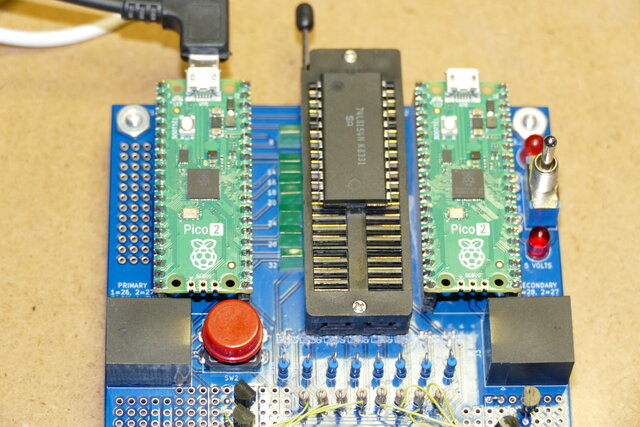
The two-PICO solution
The PICO has a lot of GPIO pins, but not quite enough to test a full 40-pin IC. The way the board is designed, you can run it on just one PICO (the "primary"), and it will fully test up to 24-pin ICs. If you need to test bigger chips, you'll need the second PICO.
Why not just add an I/O expander, like the MCP23017?
It turns out, those are actually relatively expensive, compared to what you get! For around $2.00, they give you 14 bidirectional pins (and 2 output only). But for around $6.00, you get another PICO :-)
Besides, I wanted to delve into having two PICOs talk between themselves; more of a challenge.
Hardware
Let's look at the hardware for the IC tester. We'll examine selected portions of the schematic.
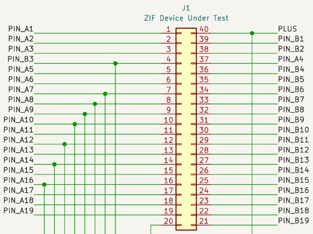
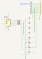
The anchor is the 40-pin ZIF socket (hover over the image for a larger view, or click on the XL to get a full size image):
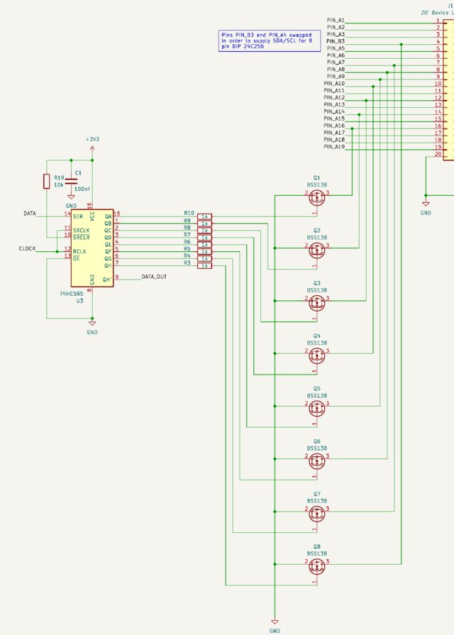
This is a crop from the full schematic, so there are wires going off to other sections. What's important to note here, however, is that pin 40 of the ZIF socket is connected to PLUS; that was the basic assumption about VCC mentioned at the start. The astute reader will notice that the pin ordering is a little "off" — where PIN_A4 should have been (if we were strictly going in order), we see PIN_B3 instead. We'll come back to that later.
For the most part, each of the PIN_xx signals connects directly to a GPIO port on one of the two PICOs. The first PICO handles PIN_A1 through PIN_A10 and PIN_B1 through PIN_B10, and the second PICO handles the rest.
It's not apparent from the schematic and the description why a single PICO configuration (with just a primary) can handle up to a 24-pin device. After all, such a device would require PIN_A11 and PIN_B11 to be connected to the primary PICO (ZIF pin 12, i.e., PIN_A12 would be the ground), but those pins are assigned to the second PICO.
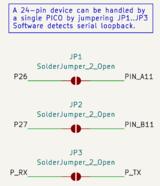
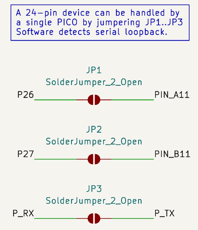
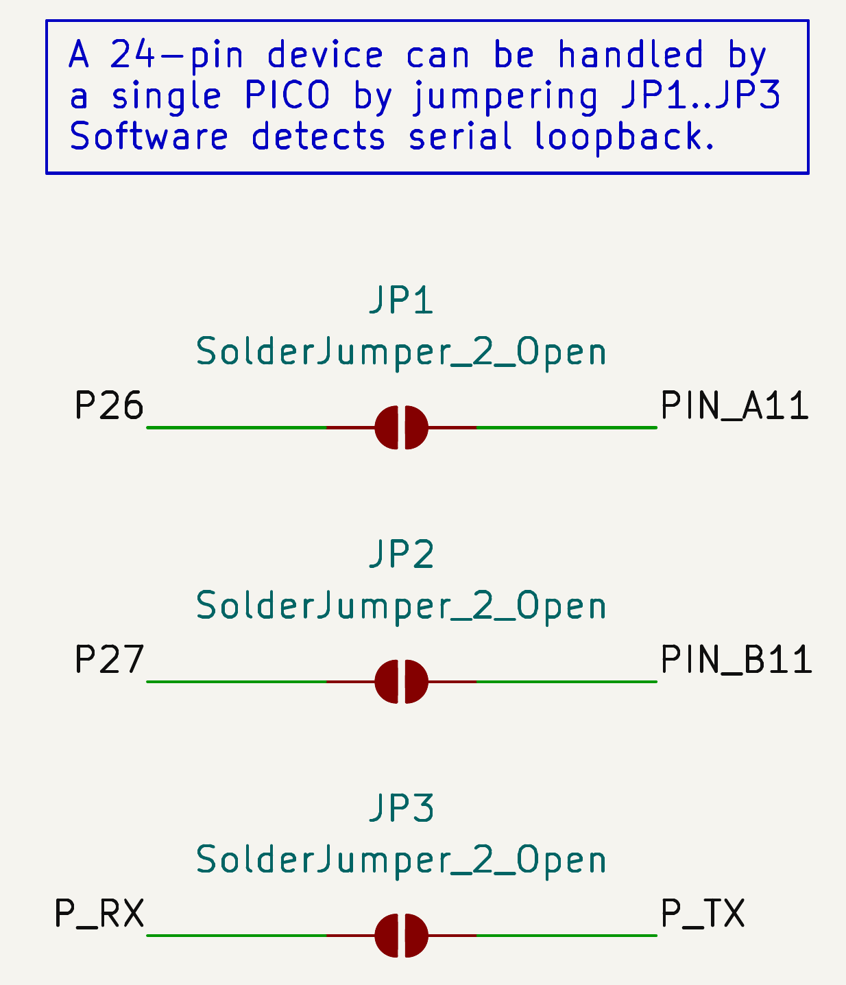
The board provides two solder jumpers that can be shorted, connecting two of the GPIOs from the primary PICO to PIN_A11 and PIN_B11. Those two GPIOs would have been used for external communications out the RJ-45, but can be repurposed for a lower-cost build.
A third solder jumper provides a loop-back, allowing the software to determine that it's in a single-PICO configuration. So, you'd jumper all three to have a single PICO handle a 24-pin device.
Connecting ground
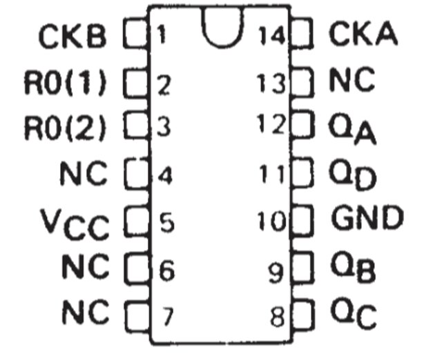
I use a 74HC595 8-bit shift register to hold the ground pin information, and BSS138 N-Channel MOSFETs to drive the ground signal:
The software clocks in 8 bits (with only one bit on, the rest off) to select one of the drivers Q1 through Q8. These then clamp the ZIF socket's pin to ground, providing sufficient power for the types of chips I'm testing.
The PLUS (VCC) circuitry is trivial; there's an SPDT centre-off switch that connects the PLUS pin to +3V3, or +5V, or nothing (if it's in the centre-off position).
That's it! That's the bulk of the hardware. For completeness, here are the two PICOs:


Hardware summary
So, turns out the hardware part was relatively simple — two PICOs provide a set of GPIO pins out to a ZIF socket, and one of the PICOs controls grounding hardware via a serial shift register and some MOSFETs.
I use the PICO-2 because it's +5V tolerant!
The software, however, is where most of the design effort went.
Software
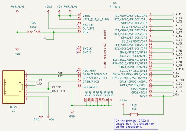
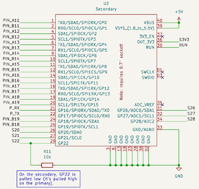
The software has some twists and turns. First off, I wanted one software load for both PICOs — I didn't want to have to build two different images, and remember which PICO I was upgrading. You'll recall the note in the PICO schematics above: "On the primary, GP22 is pulled high (it's pulled low on the secondary)."
This is a simple "who am I" trick that the software can read at startup and determine which PICO it's running on. Using a light (10k) pullup allows GP22 to be used for other functions — on the primary it serves as the DATA line that drives the 74HC595 shift register, on the secondary it goes to the expansion RJ-45.
Let's examine the software in sequential order.
Initialization
When the software starts up, it configures the GPIOs and determines if it's running as the primary or the secondary. The main() function calls init_hw():
int
main (void)
{
	stdio_init_all ();
	stdio_set_translate_crlf (&stdio_usb, false);

	while (getchar_timeout_us (1) != PICO_ERROR_TIMEOUT) ;

	init_hw ();

	if (primary) {
		menu ();		// drive processing via the menu
	} else {
		secondary ();	// wait for commands from the primary
	}
}
Within init_hw(), we figure out if we're running as the primary or secondary by examining GPIO port 22. If it's the primary, we initialize the grounding logic. In either case, spare GPIOs (gpio_primary_spares[] or gpio_secondary_spares[]) are initialized as well:
void
init_hw (void)
{
	// determine if we are primary (GP22 pulled up) or secondary (GP22 pulled down)
	gpio_set_function (22, GPIO_FUNC_SIO);
	gpio_set_dir (22, GPIO_IN);
	gpio_disable_pulls (22);
	sleep_us (5);
	primary = gpio_get (22);

	if (primary) {
		// configure grounding logic
		gpio_set_function (P_CLOCK, GPIO_FUNC_SIO);
		gpio_set_function (P_DATA, GPIO_FUNC_SIO);
		gpio_set_dir (P_CLOCK, GPIO_OUT);
		gpio_set_dir (P_DATA, GPIO_OUT);
		make_inputs (gpio_primary_spares, NELEMENTS (gpio_primary_spares));
	} else {
		make_inputs (gpio_secondary_spares, NELEMENTS (gpio_secondary_spares));
	}

	...
Next, the UART is initialized so that the two PICOs have something to talk about:
	...

	uart_init (uart0, BAUD_RATE);
	uart_set_format (uart0, 8, 1, UART_PARITY_NONE);
	if (primary) {
		gpio_set_function (P_RX, GPIO_FUNC_UART);
		gpio_set_function (P_TX, GPIO_FUNC_UART);
	} else {
		gpio_set_function (S_RX, GPIO_FUNC_UART);
		secondary_disable_tx ();
	}

	reset_hw ();

	zif_to_hal (0);										// trigger detect of standalone / loopback
}
Pins
Up until this point, it's been relatively straightforward initialization, nothing fancy. Where things get interesting is in the ZIF pin mapping. When testing a chip, we insert it "top justified", meaning pin 1 on the chip is always pin 1 on the ZIF socket. That's great for the first row of pins. The second row of pins, however, doesn't map as nicely. The chip's top right pin, regardless of whether it's pin 14, 16, 24, etc. on the chip, always lands in ZIF socket pin 40. And, to complicate things a little more (which we'll delve into in plenty of detail later), some of the pins are controlled by one PICO, and some of the pins are controlled by the other.
Pin HAL
So what I came up with is a classical Hardware Abstraction Layer (HAL)
The HAL isolates the chip testing logic from the details of two levels of mapping: chip-under-test pin to ZIF pin, and ZIF pin to PICO GPIO. The last function call you see above in init_hw() is to zif_to_hal(0), which triggers detection of whether the primary is operating stand-alone (via the loopback jumpers) or whether it's working in conjunction with a secondary.
From the point of view of the software that's testing the chip, the pins are always contiguous, and correspond to the data sheet. That is, a 14-pin device has pins 1 through 14, regardless of where they land in the ZIF socket, and which PICO controls them.
First, let's consider the zif_to_hal() function. It accepts a pin number (the 0 we gave it above is a special case, and means "no pin, just configure yourself"), and returns a hal_pin_t structure.
typedef enum {
	PICO_LOCAL,
	PICO_REMOTE,
	PICO_INVALID										// error condition
} pico_id_t;

// Opaque handle for GPIO operations
typedef struct {
	pico_id_t	pico;
	uint8_t		gpio;
} hal_pin_t;
Here we see that the hal_pin_t just encodes the PICO (local or remote) and the actual GPIO port corresponding to the requested pin. Relatively simple; until we delve into the zif_to_hal() function!
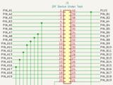
Here's the "high runner / preferred configuration" table within the zif_to_hal() function:
// this is the preferred configuration: two PICOs; supports 40 pin devices
static hal_pin_t mapping_dual [] =
{
  {L, P_PIN_A1},  {L, P_PIN_A2},  {L, P_PIN_A3},  {L, P_PIN_B3},  {L, P_PIN_A5},	// pins  1.. 5
  {L, P_PIN_A6},  {L, P_PIN_A7},  {L, P_PIN_A8},  {L, P_PIN_A9},  {L, P_PIN_A10},	// pins  6..10
  {R, S_PIN_A11}, {R, S_PIN_A12}, {R, S_PIN_A13}, {R, S_PIN_A14}, {R, S_PIN_A15},	// pins 11..15
  {R, S_PIN_A16}, {R, S_PIN_A17}, {R, S_PIN_A18}, {R, S_PIN_A19}, INVALID,			// pins 16..20 (20 == GROUND)
  {R, S_PIN_B19}, {R, S_PIN_B18}, {R, S_PIN_B17}, {R, S_PIN_B16}, {R, S_PIN_B15},	// pins 21..25
  {R, S_PIN_B14}, {R, S_PIN_B13}, {R, S_PIN_B12}, {R, S_PIN_B11}, {L, P_PIN_B10},	// pins 26..30
  {L, P_PIN_B9},  {L, P_PIN_B8},  {L, P_PIN_B7},  {L, P_PIN_B6},  {L, P_PIN_B5},	// pins 31..35
  {L, P_PIN_B4},  {L, P_PIN_A4},  {L, P_PIN_B2},  {L, P_PIN_B1},  INVALID,			// pins 36..40 (40 == VCC)
};
The mapping_dual[] array maps pins (starting at 1) to a hal_pin_t entry. For example, the first pin, pin 1, maps to {L, P_PIN_A1}. This is a hal_pin_t entry initialized with a pico value of L (which is a macro expansion to PICO_LOCAL just to keep the table size manageable) and a gpio value of P_PIN_A1 (which is a macro expansion to the value 0, representing GPIO 0). This matches up — pin 1 is indeed controlled by GPIO_0 on the primary ("local") PICO.
What about, say, pin 23 on the ZIF? The schematic shows it going to PIN_B17, which is physically connected to GPIO_13 on the secondary. Sure enough, the mapping_dual[22] (remember, we start at pin 1) entry contains {R, S_PIN_B17}, indicating an R (macro expansion to PICO_REMOTE) and a signal name of S_PIN_B17 (macro expansion to 13), which makes it GPIO_13 on the secondary ("remote") PICO.
I said that mapping_dual[] is the high runner / preferred case — there are two other cases, which I'll mention but we won't delve into.
// this is the economy version: one PICO, but with a loopback connector;
// supports 24 pin devices (note the P_26 and P_27 parts)
static hal_pin_t mapping_standalone_with_loopback [] =
{
  ... same ...
  {L, P_26},      INVALID,        INVALID,        INVALID,        INVALID,			// pins 11..15
  INVALID,        INVALID,        INVALID,        INVALID,        INVALID,			// pins 16..20 (20 == GROUND)
  INVALID,        INVALID,        INVALID,        INVALID,        INVALID,			// pins 21..25
  INVALID,        INVALID,        INVALID,        {L, P_27},      {L, P_PIN_B10},	// pins 26..30
  ... same ...
};

// this is the economy version where someone forgot to install the loopback connector;
// supports 20 pin devices
static hal_pin_t mapping_standalone_no_loopback [] =
{
  ... same ...
  INVALID,        INVALID,        INVALID,        INVALID,        INVALID,			// pins 11..15
  INVALID,        INVALID,        INVALID,        INVALID,        INVALID,			// pins 16..20 (20 == GROUND)
  INVALID,        INVALID,        INVALID,        INVALID,        INVALID,			// pins 21..25
  INVALID,        INVALID,        INVALID,        INVALID,        {L, P_PIN_B10},	// pins 26..30
  ... same ...
};
Depending on what the hardware startup / initialization detects, one of the three tables shown above is used. We'll assume it's mapping_dual[] that gets used.
So that's the first level of HAL mapping — ZIF pin number to a PICO and GPIO pair.
For completeness, here's the zif_to_hal() function (with the table contents elided for clarity):
#define	INVALID	{PICO_INVALID, 0}	// returned when a pin is not used; should never happen
#define	L		PICO_LOCAL			// GPIO is based on primary PICO
#define	R		PICO_REMOTE			// GPIO is based on secondary PICO

hal_pin_t
zif_to_hal (int pin)
{
	static hal_pin_t mapping_dual [] = { ... };
	static hal_pin_t mapping_standalone_with_loopback [] = { ... };
	static hal_pin_t mapping_standalone_no_loopback [] = { ... };

	static hal_pin_t *mapping = NULL;

	if (!mapping) {
		if (is_standalone ()) {
			if (is_loopback ()) {
				mapping = mapping_standalone_with_loopback;
				mode = "Standalone with loopback";
			} else {
				mapping = mapping_standalone_no_loopback;
				mode = "Standalone, no loopback";
			}
		} else {
			mapping = mapping_dual;
			mode = "Dual PICO";
		}
	}

	// pin numbers start at 1, all arrays are the same size
	if (pin > 0 && pin <= NELEMENTS (mapping_dual)) {
		return mapping [pin - 1];
	}
	return (hal_pin_t) { PICO_INVALID, 0 };
}
Based on the configuration (as determined by is_standalone() and is_loopback()) the static variable mapping is bound to one of the three mapping tables. Once bound, the zif_to_hal() function is just a simple lookup, returning a hal_pin_t structure.
Chip HAL
The HAL does two mappings; ZIF pin to PICO GPIO, and chip-under-test pin to ZIF pin. We've seen the first one above. The second one requires, you guessed it, more tables!
A 14-pin chip maps to the ZIF socket as follows (the "(BODY)" column is just a visual separator between the first row of pins and the second; it's where the chip body would go):
| ZIF | Chip | (body) | Chip | ZIF |
|---|---|---|---|---|
| 1 | 1 | 14 | 40 | |
| 2 | 2 | 13 | 39 | |
| 3 | 3 | 12 | 38 | |
| 4 | 4 | 11 | 37 | |
| 5 | 5 | 10 | 36 | |
| 6 | 6 | 9 | 35 | |
| 7 | 7 | 8 | 34 |
And a 16-pin chip is slightly different:
| ZIF | Chip | (body) | Chip | ZIF |
|---|---|---|---|---|
| 1 | 1 | 16 | 40 | |
| 2 | 2 | 15 | 39 | |
| 3 | 3 | 14 | 38 | |
| 4 | 4 | 13 | 37 | |
| 5 | 5 | 12 | 36 | |
| 6 | 6 | 11 | 35 | |
| 7 | 7 | 10 | 34 | |
| 8 | 8 | 9 | 33 |
The mapping function is trivial:
static uint8_t
dip_to_zif (int npins, int pin)
{
  return pin <= npins / 2 ? pin : 40 - npins + pin;
}
The function takes as input the total number of pins (e.g., 16) and the pin number that you're interested in, and returns a ZIF socket pin number.
Transport layer
At this point, we have a good understanding of how a chip-under-test pin is mapped to the ZIF socket pin. How do we actually read or write a pin?
The chip test logic doesn't want to know about the details of which PICO and which GPIO that chip's pin attaches to. It wants to express a test along the lines of "I'm testing a two-input NAND gate with inputs on pins 1 and 2, and output on pin 3". This means that the test program wants to write 0 to pins 1 and 2, and see what the output is on pin 3. Then it wants to write a 0 to pin 1 and a 1 to pin 2, and again see what the output is on pin 3. After writing all four patterns, and reading the results, the test program can then declare a pass or fail, indicating if the device does indeed behave like a two-input NAND gate.
Ultimately, each test program has access to several API functions:
- dip_init()
- dip_make_output() and dip_make_outputs()
- dip_make_input() and dip_make_inputs()
- dip_set_output() and dip_set_outputs()
- dip_get_input() and dip_get_inputs()
- dip_is_tristate()
A context structure, dip_t, holds information about the configured chip-under-test:
#define	NZIF	40

typedef struct {
	hal_pin_t	halpin [NZIF];
	const char *name [NZIF];
	int			npins;
} dip_t;
This is simply a snapshot of the hal_pin_t conversion of each pin via the HAL layer. A name can be bound to the pin (for reporting), and npins indicates the number of pins in the chip.
This is initialized by dip_init() right at the start of the test program:
void
dip_init (dip_t *dip, int npins, int ground_pin)
{
	memset (dip, 0, sizeof (*dip));
	dip -> npins = npins;
	if (ground_pin == -1) {
		gnd (npins / 2);
	} else {
		gnd (ground_pin);
	}
}
This establishes the number of pins and sets up the ground pin control (via the MOSFET hardware).
It's expected that the appropriate dip_make_input() (or the list version, dip_make_inputs()) and dip_make_output() (or dip_make_outputs()) are called to initialize the rest of the pin mappings.
Finally, the transport.
The local case is easy; dip_set_output() (or the list version, dip_set_outputs()) and dip_set_input() (or dip_set_inputs()) look at the HAL, determine that the pin is on the local ("primary") processor, and issue a gpio_put() or gpio_get() function.
If it's on the remote processor, the secondary, then a serial message is sent over the UART from the primary to the secondary, delegating the I/O work. The message is one of:
- configure GPIO pin X as input or output,
- write GPIO pin X with value Y,
- read GPIO pin X and return the value
- test GPIO pin X and return if it's tri-state or not.
Here's the dip_get_input() function as an example:
bool
dip_get_input (dip_t *d, uint8_t pin)
{
	uint8_t zif = dip_to_zif (d -> npins, pin);
	if (d -> halpin [zif].pico == PICO_LOCAL) {
		return gpio_get (d -> halpin [zif].gpio);
	}
	return cmd_gpio_get (d -> halpin [zif].gpio);
}
In the local case, it just calls gpio_get(). In the remote case, it calls cmd_gpio_get(), which creates a small message packet, sends it out the serial port, and waits for a response. When it gets the response, it returns the value.
The serial protocol
How does the serial protocol work?
Stepping back a little bit, we have a number of things to consider and work with:
- the PICO has a super high speed serial port built in (we crank it to just under 8Mbps!)
- the serial port has 16 bytes worth of buffer associated with it
- the protocol should be resilient to errors
Since we're really just sending GPIO port numbers and GPIO port values around, we're only dealing with a few bytes at most. Certainly much less than the 16 bytes of buffer that the serial ports have! This is good, because it means we can basically squirt out the entire packet in a non-blocking loop, and then collect the results at our leisure. Neither the transmit buffer nor the receive buffer will ever overflow.
So let's continue with the "gpio get" chain, and look at cmd_gpio_get():
static bool
cmd_gpio_get (int gpio)
{
	uint8_t tx [] = { 0x00, 'G', 'E', gpio, 0x00 };
	tx [0] = sizeof (tx) - 2;
	cobs_encode (tx);

	uint8_t *rx = command (tx);

	if (rx && rx [0] == 3 && rx [1] == 'O' && rx [2] == 'K') {
		return rx [3];
	}

	printf ("Unable to get remote GPIO pin value %d\n", gpio);
	return false;
}
First, we construct a small packet. We reserve the first byte with a zero for the length, and put G, E (mnemonic for "get") and the GPIO port number and another zero into the message. Five bytes total.
The first byte is set to the value sizeof (tx) - 2, which evaluates to 3. This indicates that there are three bytes of data (the G, E, and GPIO port number).
cobs_encode() puts framing bytes around our packet, and command() does a transmit-and-wait-for-reply operation.
We're expecting the remote end to have sent us a three-byte packet with O, K, and a data byte (at rx [3]) meaning that it successfully did the GPIO "get" request, and providing the data.
COBS, or Consistent Overhead Byte Stuffing, is a brilliant method of inserting framing bytes with minimal (and, as the name implies, consistent) overhead. You should read the paper from the 1997 SIGCOMM conference. It's my "go to" protocol for any work I do.
Promises
Earlier, I promised to talk about why the PIN_A4 and PIN_B3 ordering is "off". There's actually a very simple answer: to accommodate I2C testing of 8-pin EEPROM devices. By swapping the two pins, the I2C SCL and SDA lines land in the right place for the 24Cxxx family of EEPROMs. This means that (in a future version) I can use the PICO's native I2C controller to talk to the EEPROM instead of bit-banging it myself.