RMATS Card Reverse Engineering
I was curious to see how the Remote Maintenance Administration, and Test System (RMATS) card works, but didn't have any schematics.
So I reverse engineered it.
The process is simple:
- take high quality pictures of the front and back of the board
- flip the "back" picture so that it's mirrored
- use the front and back boards as Reference Images in KiCad PCB layout
Then, for each component:
- place the component in the schematic and the PCB layout
- find connections between components, updating the schematic and PCB layout
Ultimately, you'll end up with a fairly complete schematic. To finish, you'll need to buzz-out the remaining few connections using a continuity tester.
Let's look at these steps in turn.
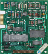
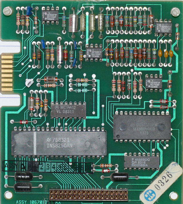
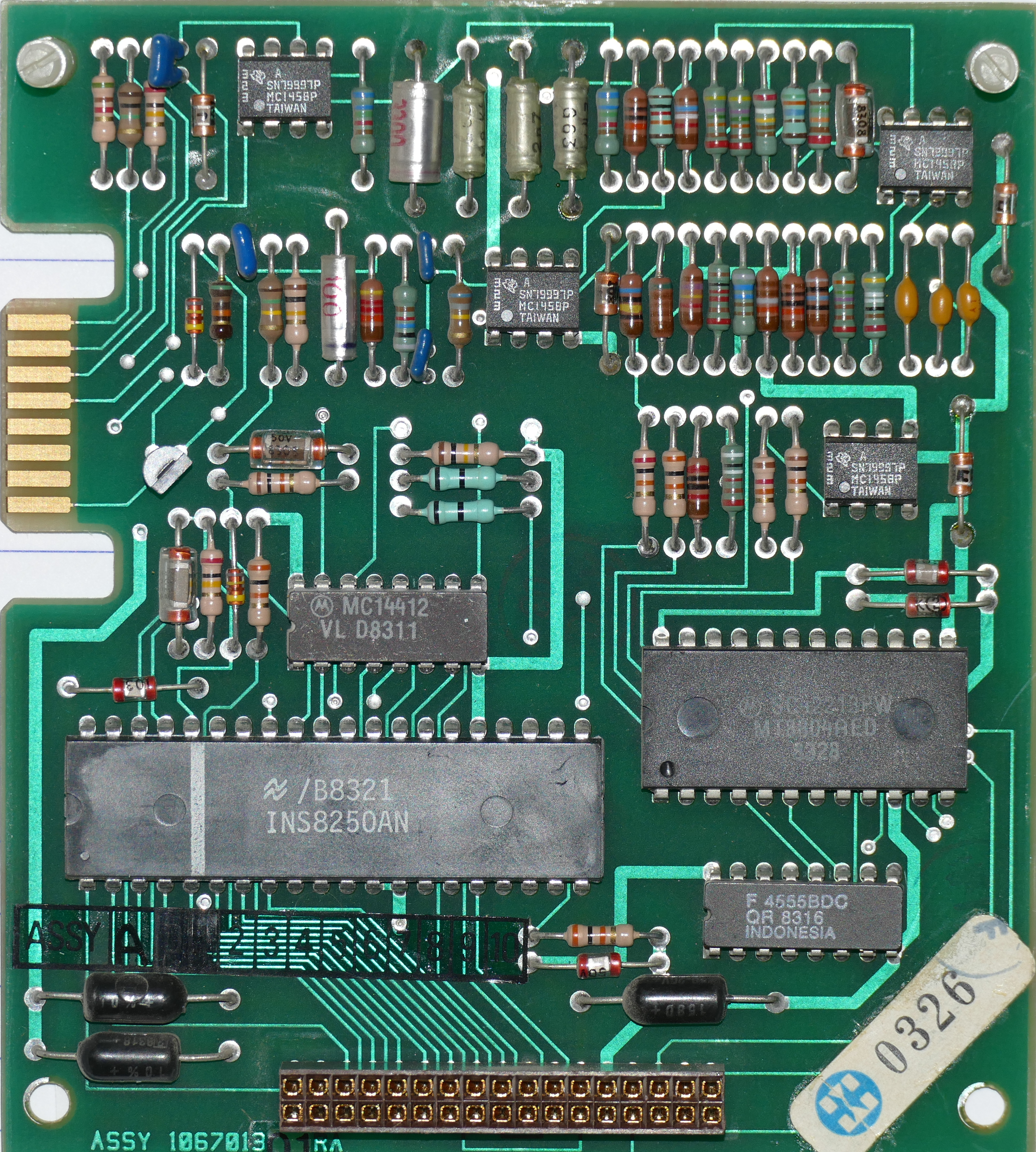
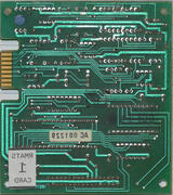
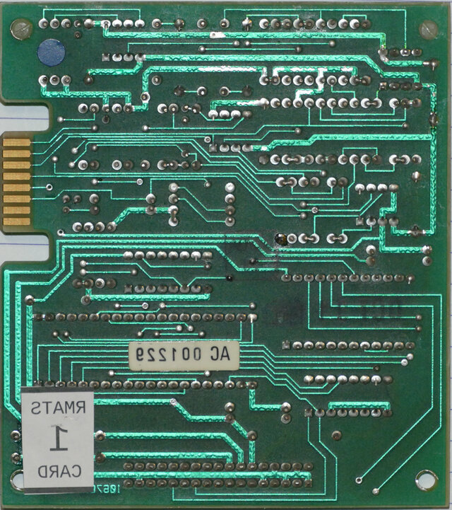
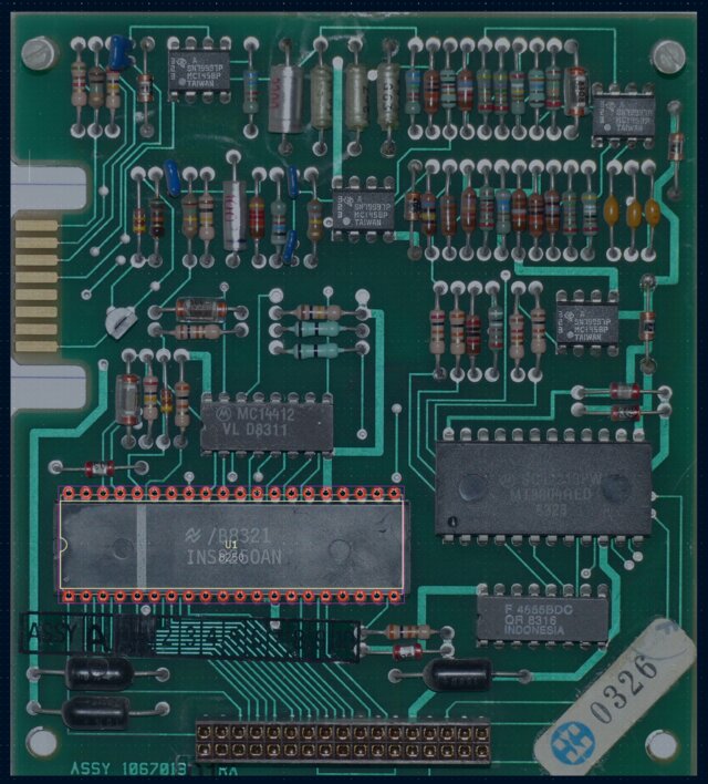
High Quality Pictures
Here are the two pictures I took; trimmed, and the back of the board (solder side) mirrored. Click on the XL to see the full camera-resolution image.
KiCad Reference Image
In the KiCad PCB editor, under the Place menu is a Place Reference Images menu item. Bring in the first board, say the front. You'll want to resize it so that it exactly matches "actual size". The easiest way to do that is to find a big component; in this case, the 8250 UART chip. It's a 40-pin package, which means that you'll have 40 pins that need to be exactly the right spacing. Easiest is to go into the Schematic editor, and plop down an 8250 chip, set it up as a 40-pin DIP package, and export it to the PCB editor.
Now you can scale the front image so that perfectly aligns with the pins of the chip.
You'll start with something like this (note the red pins for the 8250 device):
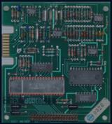
Eventually, you'll have something that looks more like this:

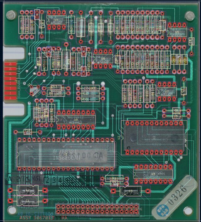
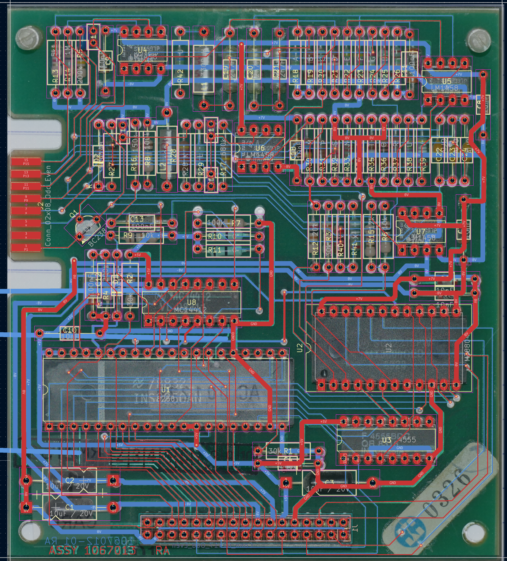
If you look closely, you'll see traces under the chips! This isn't some kind of x-ray vision, it's KiCad showing the top reference image (the component side one) and then ghosting the bottom reference image (the solder side one). As you flip between top and bottom layers, the ghosted image and the prominent image swap, allowing you to trace out lines.
Eventually, you'll have a completed PCB — you've basically traced out all the tracks on the original PCB and added them to your schematic. The red traces are the top layer, and the blue traces are the bottom layer.


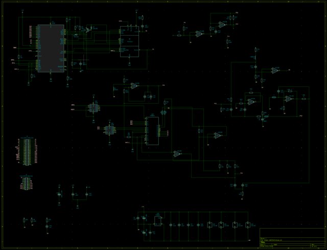
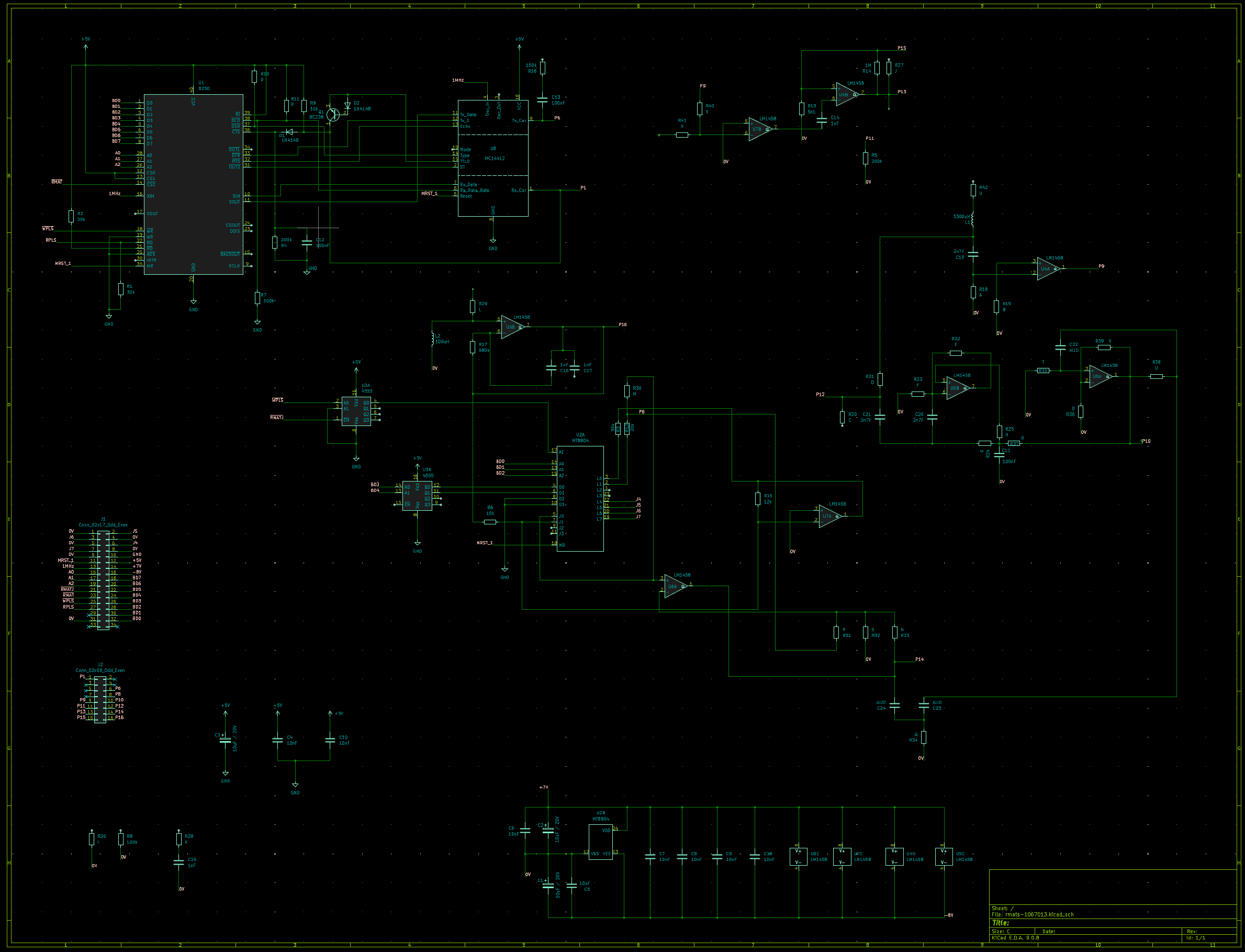
Here's what the schematic currently looks like -- I haven't finished organizing it, and I don't have values for all the 1% resistors, and there are connections missing. But this is what you get after about 2 days work: